video
2dn
video2dn
Найти
Сохранить видео с ютуба
Категории
Музыка
Кино и Анимация
Автомобили
Животные
Спорт
Путешествия
Игры
Люди и Блоги
Юмор
Развлечения
Новости и Политика
Howto и Стиль
Diy своими руками
Образование
Наука и Технологии
Некоммерческие Организации
О сайте
Видео ютуба по тегу Via In Pad Rules
Using VIA in PAD? What you need to know - Guidelines, dimensions and more ...
When to Use Via in Pad
How to Set Up Design Rules for Via-in-Pad in Altium Designer
Why is Via-in-Pad So Recommended for Routing Intricate BGA Pads?👉Get JLCPCB 6-Layer PCBs for Free!
Via-in-Pad Reliability: When Does Your PCB Need It? #pcbmanufacturing #pcbdesign
3 Key Benefits:Why Multilayer PCBs Use Via-in-Pad and ENIG #jlcpcb #engineering #pcb design
Using Vias In Pads In Your Designs
Do you know stepped hole, counterbore, crimping hole and via in pad
Via in pad
Via-in-Pad for BGA
Проектирование переходных отверстий в контактных площадках и микропереходов для HDI | Тизер вебин...
Altium Designer Tutorial 28: Altium Design rule for Via under SMD PAD.
(Sponsored) PCB Vias 101 - Phil's Lab #77
Cadence PCB DFM Pad Entry Exit Rules
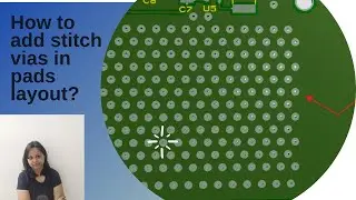
how to add stiching via in pads layout
What constitutes a Via-in-Pad? (2 Solutions!!)
Principles of PCB design, multilayer stack-ups, via in pads & copper pour zones prt3
Creating, Routing, and Using New Via Types in Altium Designer
How to do BGA fanout - VIAs & Layers
Следующая страница»